Preface
The information contained on this page is a collection of my understanding
of the AVR32 architecture. That means:
- The information might not all be accurate, I don't pretend to understand the whole thing.
- The information is not complete. I do not document everything, only the things
I am interested in. I have a very good background on the x86 architecture, so things
that are obvious to me are not detailed here either (I won't explain what Paging is used for).
Please feel free to contact me if you need more information.
Memory
NGW100 memory
The memory that is accessible from the CPU is as follow:
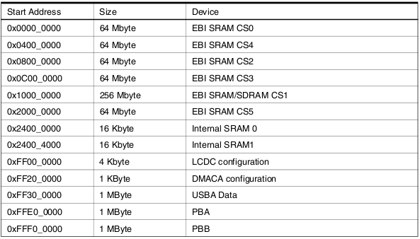
These physical address represent different memory "devices" that can be accessed by the CPU.
EBI stands for "External Bus Interface" We can see that the two 16K internal sram modules can be
accessed from address 0x24000000 and 0x24004000.
The NGW100 board does not have that much memory devices on it, therefore the CPU
has some "slots" it cannot access since no devices are attached to it. The NGW100 contains the following:
| Memory | Device type | device |
|---|
| 0x0000_0000 | EBI SRAM CS0 | parallel flash(8MB) |
| 0x1000_0000 | SDRAM CS1 | SDRAM chip(32MB) |
| 0x2400_0000 | Internal SRAM0 | CPU Internal SRAM0(16k) |
| 0x2400_4000 | Internal SRAM1 | CPU Internal SRAM1(16k) |
We can see that it would be possible to add more memory if we were to connect more flash or SRAM chips
on the EBI.
The NGW100 also contains a 8MB serial flash chip but that chip is not accessible by the EBI. It is connected
to the SPI bus. NGW100 has two SPI buses, the serial flash is on bus 0 (SPI0) So in order to access that
memory, one would need to write a driver. The Serial dataflash can be seen as the hard drive in that case.
Virtual memory
When accessing a memory location, the address is always a virtual address, meaning that it isn't necessarily
mapped exactly at the same areas on the physical addressing. There are 2 kinds a virtual memory schemes:
Segment translation and Paging. By default, after reset, segment translation is enabled.
The virtual space is divided in subsections that we will call "segments" in this document. Each segment
is designed to be accessed by some privileged mode. Here is the layout
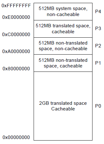
It is possible to use segmentation and paging at the same time. This is
covered in the AVR32 architecture document at page 32. Using both modes
results in having P1 and P2 constantly mapped to 0x00000000 and that mapping
cannot change. P0 and P3 can be remapped accordind to the page translation
table (TLB). Again, P4 is mapped to 0xE0000000 and is used for memory-mapped
IO.
When designing a kernel, it would be a good idea use P1 since it will always map
to physical location 0x00000000 regardless of the TLB. P1 is only
accessible by priviledged code. So by re-mapping P0 somewhere else, physical
location 0x00000000 would be accessible by P1 and P2 only so application code
would not be able to access it. The choice of P1 over P2 is because P1 is
cacheable. From what I understand, using cached memory would be usefull
for data more than for code. Cacheable memory will increase performance if the same memmory
accessed several time. By putting code that execute once, we waste cache space. The
first application I did made an LED blink on the board. You could see a BIG performance
increase by running the code from P1 instead of P2 because the code being executed
was a loop making a led flash, so in that case, putting the code in P1 had great benefits.
If you have an opinion on that, please feel free to share this with me.
Segment translation
when using segment translation, the segments P0,P1,P2,P3 are all translated to physical address
0x0000_0000. P4 is used for memory mapped IO. Therefore, accessing address 0x80000000 or 0xA0000000
or 0xC0000000 will take us to physical location 0x00000000, being the begining of the parallel flash memory on the NGW100.
Paging
Pages can be 1,4,64 or 1024K in size. A table entry defines the mapping to
the physical location and the access rights associated to that chunk of memory.
When remapping the memory, it is possible to have a system-wide mapping, or
have a mapping for each process running on the CPU. The later is called Private
Virtual Memory. This mode will be described.
The operating system must maintain a page table. In the case where 4K pages are used and a total
of 32meg of memory is available, 8192 page entries would be needed. A page entry is 32bit wide.
The page lookup differs from the one from the x86 architecture because it is not automatically done.
When accessing memory, the CPU determines the page number of the address according to the page size.
When it has determined the page number, it looks in the TLB for a matching entry. The TLB is a table
that contains 64 page entries. This table is not located in RAM but in the MMU itself. After
the OS has booted and set up the paging mechanism, the TLB will be empty. When the OS will
try to access a translatable location (address within P0,P3) it will iterate trough its TLB
but will find no match. A TLB miss exception will then be issued. The exception handler will need to
look at the TLBEAR register, which contains the virtual address that caused the fault. With that
address, the handler will be able to load correct table entry in the TLB by preparing the 32bit
field and loading it with the tlbw instruction. On the next memory access, the table entry will
already be in the TLB and no exception will be issued. Of course, after some time, the TLB will
contain 64 entries as new entries are cached in the TLB, old entries will be overwritten.
In order to load an entry in the TLB using tlbw, the TLBEHI and TLBELO registers must be set.
The exception handler will copy the contents of its page table entry in TLBELO, set TLBEHI and
execute tlbw to update the TLB. The index of the TLB entry is managed by hardware. The
adress of the page table can be stored in the PTBR register but it does not seem to be mandatory.
This seems to be provided for convenience only.
In reality, there are two TLBs: one for instruction access and one for data access. If the
instruction that tries to access memory is trying is data access, the DTLB miss exception
is issued, otherwise it is the ITLB exception. Depending on the exception, some fields in
the TLBEHI register need to be set differently. This allows the system to have a total
of 128 entries.
So basically, these are the operations that are performed:
- Setup page table entries. A table residing in ram that contains all necessary entries
to load in the TLBELO register
- Page size is determined to be 4k
- An application (or kernel) makes an access to memory 0x00005100
- The page number is determined to be 5 (offset of 100)
- The MMU searches trough the TLB for page #5
- A TLB miss exception is issued because that page is not cached in the TLB yet
- The exception handler loads TLBELO from the page table. It finds the correct entry
because the virtual address is stored in the TLBEAR register. It knows where to find page #5.
- Setup TLBEHI properly
- Execute tlbw
- The page entry is written in the TLB at an index determined by hardware.
- Normal flow of execution is resumed and memory translation is performed, allowing the application
to access the memory previously addressed.
memory protection
Even though the parallel flash memory is directly accessible trough the address space, it is not
possible to write to directly. Before writing to the memory, a full sector must be erased. On
the ngw100, the parallel flash is divided into 135 sectors of 32k and some are 4k.
Private virtual space
This part is not so clear in the architecture document. The main concept is that when running several process at
the same time, the OS should assign a unique ID to each process. as soon as (or right before) the process
has changed du to a task-switch, the process ID should be written in the ASID field in the TLBEHI register.
So when an TLBMiss expcetion occur, this field is already set when loading the page into the TLB. But
the important thing is that on a TLB lookup, the MMU will compare the ASID field in the TLB entries with
the ASID currently loaded in TLBEHI.. It took me some time to figure that last one out. So the
ASID field in TLBEHI has two purposes: 1) to inform the TLB what ASID the new page should be tagged with
when using TLBW and 2) to inform the TLB what is the current ASID used by the current process.
It really is the same thing though when you think about it.
Dirty bit
The dirty bit in the page table entries is not set automatically by hardware. Instead, when the dirty
bit is cleared and a store instruction is used to access that page, a DTLB modified exception is
issued. It is up to the exception handler to set the bit. To do this, it must find the page entry
in its table, modify the bit and load it back to the TLB using the tlbw instruction. Before executing
tlbw, the MMUCR[drp] index must be set appriately in order not to have duplicate entries in the TLB
The dirty bit could
be used to implement swapping to disk but I do not feel that this is usefull on the NGW100. Therefore,
the dirty bit should be set when filling the TLB in order to get the Modified exception off our way.
Code execution
The CPU can execute code located anywhere in the addressing space. Executing code directly from the NGW100's
serial dataflash is therefore impossible since it does not reside in the addressing space. Although execution can happen
anywhere, if using the SDRAM memory, one must initialize the SDRAM controller before accessing that memory space.
Upon reset, the program counter (PC) is set to 0xA000_0000 and the first instruction to be executed is at that address.
Since the CPU is in segment translation mode, that address is translated to physical address 0x0000_0000 which is the address
of the parallel flash in our case (see upper table). Therefore, the "boot sector" is located at the begining of the parallel flash memory
Clock speed
The CPU can run on two different clocks: OSC0 and PLL0. OSC0 is attached to the 20mhz crystal on the board. This
is the default used when the CPU is reset. Using PLL0, the clock gets divided and the CPU can run at up to 150MHZ.
Increasing the clock speed allows you to increase the SDRAM refresh rate too. The sdram can run at half the speed of the master. So
if running the main clock at 150MHZ, then make sure to increase the SDRAM at 75MHZ. If it is slower, it shouldn't cause any problem
(I think... I did not test that).
    /* set system clock */
    mov     r0,AVR32_PM_ADDRESS
    lddpc   r2,.pllconfig
    st.w    r0[AVR32_PM_PLL0],r2

    /* wait for PLL to be locked */
1:  ld.w    r2,r0[AVR32_PM_ISR]
    bld     r2,0
    brne    1b

    /* set main clock to PLL*/
    mov     r2,2
    st.w    r0[AVR32_PM_MCCTRL],r2

    /* set full clock to PBA,PBB and CPU. HSB=CPU/2 */
    mov     r2,0x8000
    st.w    r0[AVR32_PM_CKSEL],r2
It is important to clear CKSEL because it seemed to be set by u-boot. By doing that, we are telling the CPU
that PBA,PBB and the CPU should run at Frequency/1. Since the USART receives its clock from PBA,
we can calculate of baud rate based on 150MHZ now. In order to have SDRAM work correctly, HBS
speed is set to half the speed of the PLL. this is done by writting 1 to bit15 of AVR32_PM_CKSEL.
SDRAM
When doing standalone developpement, the SDRAM controller must be initialized before we can start to use that memory. I couldn't
find much information on the subject. There is a lot of code out there (mainly for the stk1000 though) but there isn't
really any information that describe why the code works that way. So I ended up looking at the u-boot source code and I
did the exact same thing except I have translated in in ASM. I was unable to test it though because I am booting
with u-boot for the moment, so the SDRAMC is already initialized. I don't know if it is because my code is working
or if it is because it was already OK before starting to use it. My guess is that if my code would be wrong, it
would have screwed up the controller. So here is a bit of code that I translated from the u-boot source code.
/************************
* SDRAM Initialization
************************/
sdram_init:
    stm     --sp,r7, lr

    // disable the pull-up resistor for the SDRAMC SFR4 in the HMATRIX controls that (datasheet, page 87)
    lddpc   r6,.hmatrix
    mov     r8,0x0002;                          // SDRAMC chip select
    ld.w    r9,r6[AVR32_HMATRIX_SFR4]
    or      r9,r8
    st.w    r6[AVR32_HMATRIX_SFR4],r9
    mov     r8,0x0100;                          // Disable pullup
    or      r9,r8
    st.w    r6[AVR32_HMATRIX_SFR4],r9

    // initialize data bus bits 31-16
    lddpc   r6,.pioe
    mov     r8,0xFFFF;
    ld.w    r9,r6[AVR32_PIO_ASR]
    and     r9,r8
    st.w    r6[AVR32_PIO_ASR],r9
    ld.w    r9,r6[AVR32_PIO_PDR]
    and     r9,r8
    st.w    r6[AVR32_PIO_PDR],r9

    // setup sdram info
    lddpc   r6,.sdramc
    lddpc   r9,.sdraminfo
    st.w    r6[AVR32_SDRAMC_CR],r9

    // send a NOP to start clock
    lddpc   r8,.sdrambase
    mov     r9,1                    // MODE_NOP
    st.w    r6[AVR32_SDRAMC_MR],r9
    ld.w    r9,r6[AVR32_SDRAMC_MR]  // dummy read
    mov     r9,0
    st.w    r8[0],r9

    // wait a while
    mov     r9,40*200
sdramDelay:
    sub     r9,1
    brne    sdramDelay

    // Precharge All command is issued to the SDRAM
    mov     r9,2                    // MODE_PRECHARGE
    st.w    r6[AVR32_SDRAMC_MR],r9
    ld.w    r9,r6[AVR32_SDRAMC_MR]  // dummy read
    mov     r9,0
    st.w    r8[0],r9

    // Provide eight auto-refresh (CBR) cycles
    mov     r9,4                    // MODE_AUTOREFRESH
    st.w    r6[AVR32_SDRAMC_MR],r9
    ld.w    r9,r6[AVR32_SDRAMC_MR]  // dummy read
    st.w    r8[0],r9
    st.w    r8[0],r9
    st.w    r8[0],r9
    st.w    r8[0],r9
    st.w    r8[0],r9
    st.w    r8[0],r9
    st.w    r8[0],r9
    st.w    r8[0],r9

    // CAS from info struct, burst length 1, serial burst type
    mov     r9,3                    // MODE_LOAD_MR
    st.w    r6[AVR32_SDRAMC_MR],r9
    ld.w    r9,r6[AVR32_SDRAMC_MR]  // dummy read
    mov     r9,0
    st.w    r8[0x0],r9

    // A Normal Mode command is provided, 3 clocks after tMRD is met.
    mov     r9,0                    // MODE_NORMAL
    st.w    r6[AVR32_SDRAMC_MR],r9
    ld.w    r9,r6[AVR32_SDRAMC_MR]  // dummy read
    mov     r9,0
    st.w    r8[0x0],r9

    // Write refresh rate into SDRAMC refresh timer count register
    mov     r9,(156 * (SDRAM_HZ / 1000)) / 10000
    st.w    r6[AVR32_SDRAMC_TR],r9

    ldm     sp++, r7, pc


dataj: rjmp dataj   // to make sure we don't execute code

.sdramc:        .int AVR32_SDRAMC_ADDRESS
.pioe:          .int AVR32_PIOE_ADDRESS
.hmatrix:       .int AVR32_HMATRIX_ADDRESS
.sdrambase:     .int 0x10000000
.sdraminfo:     .int    ((1 << AVR32_SDRAMC_CR_NC )\
                        |(2 << AVR32_SDRAMC_CR_NR )\
                        |((1) << AVR32_SDRAMC_CR_NB )\
                        |(3 << AVR32_SDRAMC_CR_CAS )\
                        |(4 << AVR32_SDRAMC_CR_TWR )\
                        |(14 << AVR32_SDRAMC_CR_TRC )\
                        |(2 << AVR32_SDRAMC_CR_TRP )\
                        |(2 << AVR32_SDRAMC_CR_TRCD )\
                        |(14 << AVR32_SDRAMC_CR_TRAS )\
                        |(1 << AVR32_SDRAMC_CR_DBW)\
                        |(20 << AVR32_SDRAMC_CR_TXSR ))
Note that this is for the ngw100 board only. Other boards may have different SDRAM chips/clock speed/buse size and would require a different
configuration. The SDRAM_HZ constant should be defined to whatever the HBS speed you are using. Usually this would be
half the CPU speed, and you should have configured that when setting up the PLL. In my case, this is 75MHZ because my CPU runs at 150MHZ. for the NGW100's SDRAM here are some value that you need:
| Parameter | Value |
|---|
| Rows | 13bit |
| Cols | 9bit |
| CAS | 3 |
| Banks | 4 |
| DBW | 16bit |
| txsr | 133.3ns |
| tras | 93.1ns |
| trcd | 40ns |
| trc | 93.3ns |
| trp | 40ns |
| twr | 26.6ns |
The Configuration Register of the SDRAMC must loaded with these values. See page 552 of the datasheet
to determine how to load those values. The last 6 parameters in the table were taken
from an example code. These timigs are in nanosecods, but the configuration register must
be loaded with a number of cycles. So if you are running at 150MHZ, one cycle = 1/150M = 6.6ns.
if txr is supposed to be 133.3, then this would be 20 cycles.
Interrupts
When the CPU encounters an error, it issues an exception. A table containing entry points for all exceptions handlers
must be defined. This table is called the EVBA. It is very similar to the interrupt vector table
on the x86 architecture. One thing that is VERY important to know is that the EVBA must start on a 8kb
boundary. If it isn't, you can get a lot of strange problems. The easiest way to do this, is to
define the EVBA at the begining of the code so that when booting, EVBA+0x00 will be executed. Since EVBA+0x00 is
the entry for "Unrecoverable Exception", the software may take a look in the status register to see if
the CPU is in Exception mode. If it isn't, then we know that this is because we are booting so we should
jump to the bootstrap.
Initialising the EVBA is just a matter of writting the base address (EVBA+0x00) to the EVBA system register.
lddpc   r8,evbaconstant
mtsr    AVR32_EVBA,r8
evbaconstant: .int EvbaBaseEntryPoint
IRQ
Before going any further, make sure that INTC is enabled in PBBMASK (See Power Manager section of the datasheet).
The documentation in the datasheet about INTC is not very clear. The application note AVR32101 is erroneous (errors in figure 3 and 4)
and the code examples provided are very confusing.
Devices such as the USART, SPI and timer (and many others) can trigger interrupts. To do so, they are attached to the INTC with
an interupt request line. If we take the timer interrupt for example, we can find in the header files that AVR32_TC0_IRQ = 704.
The INTC supports 64 interrupt groups with 32 lines in each group. Each group can be assigned a priority from 0 to 3.
An IRQ belongs to group (IRQ/32) and attached to line (IRQ%32). TCO_IRQ/32 = 22, and TC_IRQ%32 = 0, so TC0_IRQ
is the first line in group 22. To be able to handle those events, we would need to declare a handler right after the end
of the EVBA and fill IPR22 with the relative adress of the handler (intGrp22_address - evba_base_address). We would
then need to set the proper int level in IPR22 (can be whatever you like) as well. That handler will receive events
for all 32 lines in the group. If only one device was setup to trigger interrupt, this is fine. But if another
device was setup to trigger an interrupt in the same group, then the handler would need to look at the IRR22 register
in order to determine what line has triggered that event.
evbabase:
ex0:    bral ex0Handler
ex1:    bral ex1Handler
....
ex0x100:    bral ex0x100Handler
intGroup22:
    // This handler is called because one IRQ between 704 and 735 triggered
    // check IRR to know which IRQ triggered.
    // process IRQ
    rete
    // initialize INTC
    mov     r8, (intGroup22-evbabase)                 // set offset
    sbr     r8,31                                   // set level to INT3
    sbr     r8,30                                   // set level to INT3
    lddpc   r9,.INTC
    st.b    r9[INTC_IPR22],r8
    ....

    .INTC: .int 0xFFF00400
Depending on the device that triggered the interrupt, it might be necesary to clear the interupt request. This is device dependant,
so you should read on that. For example, the USART generates an interrupt but as soon as you read a byte from it, it clears
its interrupt flag automatically so you don't need to do it. This might not be the case for other devices though.
Shadow Registers
Page 24 of the ap7000 datasheet shows the register set in different context. The gray squares indicate
that the register is shadowed. If we take the INT3 context for example, we see that r12 is shadowed.
This means that when entering the context, the CPU saves r12 in R12_INT3 and restores it when leaving the context.
In that case, we don't have to push r12 onto the stack if we use it in the handler. If you take an Exception,
you see that no general purpose registers are shadowed, therefore you need to push/pop them on the stack
if you use them in order not to disrupt the interrupted code.
Multi-threading
Assuming that applications run in "application mode" and timer interrupt handler runs in "INT3 mode", it is
very easy to do task switching. When entering INT3 mode, registers from r8 to r15 are shadowed. Changing those
registers won't matter since they will be restored by hardware before going back to application mode. The STMTS
instruction allows us to save the content of registers r0-r14 in memory. The good thing
about this instruction is that it will save the content from the application-mode register. So if
"r8" was modified in the INT3 mode handler, this value will not be saved but instead it will be the value
from application mode. By saving those registers, it is possible to do safe task switching but two more
registers must be saved: INT3_RAR and INT3_RSR. INT3_RSR needs to be saved because it is the content of the
status flags register before swithing to INT3 mode. INT3_RAR contains the address that the handler must return
to. These pretty much all the registers you need to take care of.
Serial flash
Before continuing, you should understand how SPI works.
The serial flash chip on the NGW100 is a AT45DB642D. It is connected to the SPI bus 0, CS0 of the CPU. It is supposed
to be able to run at 66MHZ but atmel suggest to use it at 20MHZ. The first thing you need to do is to have a working SPI setup. I think it is pretty straight-forward to uderstand it from the datasheet but here is some code that
will save you a lot of time trying to understand the framework examples:
dataflash_init:
    stm     --sp,r8,r9,lr

    lddpc   r8,.spi0

    /* reset SPI0 */
    mov     r9,0b10000000
    st.w    r8[AVR32_SPI_CR],r9

    /* set Master, use CS0, MCK = PBA/1 = 150MHZ*/
    mov     r9,0x0013
    st.w    r8[AVR32_SPI_MR],r9

    /* configure chip select */
    mov     r9,0x0809              // MCK/8 = 18.5MHZ , stay active. Atmel suggest going no more than 20MHZ
    orh     r9,0x0000
    st.w    r8[AVR32_SPI_CSR0],r9

    // Assign pins to SPI
    mov     r9,(1<<AVR32_SPI0_SCK_0_PIN)|(1<<AVR32_SPI0_MISO_0_PIN)|(1<<AVR32_SPI0_MOSI_0_PIN)|(1<<AVR32_SPI0_NPCS_0_PIN)
    lddpc   r7,.pioa

    st.w    r7[AVR32_PIO_PDR],r9        // disable GPIO control
    st.w    r7[AVR32_PIO_ASR],r9        // peripheral A
    st.w    r7[AVR32_PIO_PUDR],r9       // pull-up disable


    /* enable SPI0 */
    mov     r9,1
    st.w    r8[AVR32_SPI_CR],r9

    ldm     sp++,r8,r9,pc

.pioa: .int AVR32_PIOA_ADDRESS
.spi0:  .int 0xFFE00000
//////////////////////////////////////////////
/// write SPI
/// INPUT: r6=byte to send
/// OUTPUT: r12=byte that was shifted in during write
/////////////////////////////////////////////
writeSPI:
    stm     --sp,r7,r9,lr


    lddpc   r9,.spi0


    st.w    r9[AVR32_SPI_TDR],r6

1:  ld.w    r7,r9[AVR32_SPI_SR]
    bld     r7,AVR32_SPI_TXEMPTY_OFFSET
    brne    1b

    ld.w    r12,r9[AVR32_SPI_RDR]

    ldm     sp++,r7,r9,pc
dataflash_readmanufacturer:
    stm     --sp,r6,r8,r9,lr

    mov     r6,0x9F
    rcall   writeSPI

    rcall   writeSPI // send dummy byte
    mov     r8,r12
    rcall   debug_showRegister

    rcall   writeSPI // send dummy byte
    mov     r8,r12
    rcall   debug_showRegister

    rcall   writeSPI // send dummy byte
    mov     r8,r12
    rcall   debug_showRegister

    sbr r6,24                                   // end of transmission
    rcall   writeSPI // send dummy byte
    mov     r8,r12
    rcall   debug_showRegister

    ldm     sp++,r6,r8,r9,pc
Dataflash
Now that you can access the dataflash with the SPI bus, here is some theory about the dataflash chip itself.
To use the dataflash, you simply need to send an "command" byte followed by parameters and data. I will
describe the commands I am using. Before starting, it is important to understand:
- the dataflash has two type of memory: Buffer, and Main memory. The buffer is an internal sram and the main memory is the flash itself.
- The smallest unit that can be read/written/erase is a page, and is 1056 bytes in size.
- There are other units (Sectors and Blocks) but I don't care much for those right now.
- A page read is done by reading the page directly from main memory
- A page write can be done many ways, but the way I prefer is: send bytes from MCU to dataflash's SRAM buffer,
compare buffer content to the page we are about to change, if buffer is different, copy buffer to page in main memory.
When we need to send a page address to the chip, this is done by sending 3 bytes containing the page number
and the offset in that page. In my case, I always use an offset of zero since I want to read the whole page.
The 3 bytes need to be sent the following way:
| Byte 0 (MSB..LSB) | byte 1 (MSB..LSB) | Byte 2 (MSB..LSB) |
|---|
| Page Num Bit12 |
Page Num Bit11 |
Page Num Bit10 |
Page Num Bit9 |
Page Num Bit8 |
Page Num Bit7 |
Page Num Bit6 |
Page Num Bit5 |
Page Num Bit4 |
Page Num Bit3 |
Page Num Bit2 |
Page Num Bit1 |
Page Num Bit0 |
Offs Bit10 |
Offs Bit9 |
Offs Bit8 |
Offs Bit7 |
Offs Bit6 |
Offs Bit5 |
Offs Bit4 |
Offs Bit3 |
Offs Bit2 |
Offs Bit1 |
Offs Bit0 |
Read status
By sending command 0xD7 to the chip, every subsequent dummy bytes sent to the chip will return us the status of
the chip. As long as the chip is selected (CS is low), sending the dummy byte will return an updated status byte.
So when polling the chip, we only need to send 0xD7 once, and send dummy bytes until the desired status is seen.
0xD7,dummy
Read page from main memory
You need to send the command byte, 3 address bytes, 4 dummy bytes and every subsequent dummy byte will return the bytes stored in the page.
0x87,addr0,addr1,addr2,dummy0,dummy1,dummy3,dummy4,data0,...,data1055
Write to buffer
This will write the your data in the internal SRAM buffer of the dataflash.
You need to send the command byte, 3 address bytes, and every every bytes that need to be stored in the page.
0xD2,addr0,addr1,addr2,data0,data1,...,data1055
Compare buffer to main memory
With this command, we simply instruct the dataflash chip to compare the contents of the buffer to a page
in main memory. This allows us to determine if we should erase/write the page. It would be a waste
to write the page if it has not changed.
0x61,addr0,addr1,addr2
After that, we can proceed with polling the chip for the status register until the RDY flag is set
write buffer to memory with built-in erase
With this command, we instruct to dataflash to take the contents of the SRAM buffer, and copy it to the main page.
0x86,addr0,addr1,addr2
After that, we can proceed with polling the chip for the status register until the RDY flag is set
Ethernet
The AP7000 has an embeded MAC module. The PHY is handled by a second chip (DP83848I) on the NGW100. There are two RJ-45 jacks and
two PHY chips on the board. Before continuing, here is some information that can be usefull for later use:
| PHY ID | IRQ group | RMII pins | MII PINS | |
| ETH0 | 1 | 25 | PIOC, DEV-A | PIOC, DEV-A | |
| ETH1 | 3 | 26 | PIOD, DEV-B | PIOC, DEV-B | |
Buffers
I won't go into the details here since this is very well explained in the datasheet. Basically, you need to allocate space for receive
buffers and send buffers. Each receive buffers are 128bytes long and TX buffers are 512 bytes long. Of course, one receive packet
will span accross several receive buffers most of the time. The AP7000 must know where those buffers are located. for this,
a list of descriptors must be created. This is another buffer in memory that contains a list of 64bit entries containing
properties such as the location of each buffers (1 entry per buffer). The pointer to the descriptor list must then be given
to the MAC module. It is the same concept as the segment descriptors on the i386. It is important to use physical addresses
in descriptors and in RBQP and TBQP.
Initialization
MAC
First thing to do is to determine if you want to use RMII or MII communication. RMII requires less pins on the chip but requires a higher
clock rate. In my case, I chose to use MII. For MII, all MACB related pins must be disabled in the PIO. A quick look at pages 84,85 of the
datasheet will show you what pins need to be configured. Basically, you want to tell the MCU that those pins will be controlled
by the MACB and that they are NOT general purpose pins. This will cause conflicts with the LCDC pins though.
After that, you need to load the MAC address, setup the descriptor tables and enable the transmitter/receiver.
PHY
By looking at my source code, you will see that the PHY initialization is very easy. This process allows you
to select auto-MDX mode, select LED modes and the link speed. In my case, I only advertise 100mbps FD during auto-negotiation.
The steps are: Enable auto-MDX, start auto-negotiation, and wait for link status to be up. Note that when setting auto-negotation, this will tell the chip to do auto-negotiation everytime it detects a cable plugged in. So it is not necessary
to re-init the PHY everytime a cable is plugged in. You configure it once and it is good to go for as long as you leave
the power on.
The PHY can be configured to generate an interrupt on an output pin when the link status changes. The AVR32 chip can detect this
by triggering on a pin change interrupt. Unfortunately, the PHY INT pin is not connnected on the AVR32 on the NGW100 so it is
impossible to detect this.
LCD Controler
The ap7000 has an integrated LCDC. The LCD I am using is a Hitachi TX14D12VM1CBB (TFT)
Wiring
If you look at the pinout of the ap7000, you will notice that some of the LCDC pins are duplicated. This
is because each pin has a dual function and this duplication allows us to avoid possible conflicts. In my
case, I want to be able to use the MACB1 device but the pins are shared with the LCDC. You can use the PIO
to specify that, for example, pin PC26 be assigned to peripheral B. In that case this would be MACB1_TX_ERR.
For more information on peripheral selection, see section 9.7 in the ap7000 datasheet. So if PC26 is used for MACB,
then what do we do in order to use LCDC_DATA0? Lucky for us, that function is also available on PE03. Since
the NGW100 uses 16 lines to access the sdram, PE0 to PE15 do not need to be assigned to peripheral A, so we
can use peripheral B, the LCDC. Another major reason why we would use those pins is because they are broken out
on header J7 on the NGW100.
Some people say that on the NGW100, the SD card could conflict with the LCDC. This is because the pin that
triggers an interrupt when an SD card is inserted is connected to pin LCDC_PWR. That pin is supposed power
the LCD. We won't use that pin and we can set it as a GPIO so that the LCDC won't use it. The VDD connections
of the LCD will instead be connected on the 3.3V pin of the J7 header.
The DTMG pin on the LCD is a "Data valid" pin. It replaces HSync and VSync. This needs to be connected
on the DVAL pin of the ap7000
The following is a table showing the connections between the Hitachi TX14D12VM1CBB and the J7 header on the
NGW100. Note that this is of 16bit colors only.
| J7 pin | LCD pin | LCD pin name | AP700 pin name |
|---|
| 33 | 1,2,3,4 | VDD | - |
| 34 | 7,9,11,15,19,23,27,31,36, | VSS | - |
| 25 | 6 | DTMG | PE01 |
| 28 | 8 | DCLK | PC21 |
| 5 | 33 | R1 | PE07 |
| 6 | 32 | R2 | PC31 |
| 7 | 30 | R3 | PD00 |
| 8 | 29 | R4 | PD01 |
| 3 | 28 | R5 | PE05 |
| 12 | 26 | G0 | PE11 |
| 13 | 25 | G1 | PE12 |
| 14 | 24 | G2 | PD07 |
| 15 | 22 | G3 | PD08 |
| 16 | 21 | G4 | PD09 |
| 4 | 20 | G5 | PD06 |
| 21 | 17 | B1 | PE17 |
| 22 | 16 | B2 | PE18 |
| 23 | 14 | B3 | PD16 |
| 24 | 13 | B4 | PD17 |
| 19 | 12 | B5 | PE15 |
Initialization
The LCDC uses two clock sources. The first one is the one we enable in the HSB MASK in the Power Manager
This is done the same way as we do for any other devices like MACB, PBB, PBA etc..
The second one is the clock that will be used by the LCD constroller core and drive the pixel clock.
This clock is refered to as the LCD Core Clock in the datasheet. If you look at the Power Manager
section in the datasheet, you will notice that they talk about Generic Clocks. The LCD Core Clock is sourced
by the Generic Clock #7. You need to configure the GCCTRL7 register in the Power Manager to enable it
and choose whether the PLL or the OSC will be used as for this generic clock. My PLL is 150MHZ, but
the datasheet mentions that "When the LCDC is being used in a system with SDRAM, the SDRAM clock frequency
must be greater than the frequency of the LCDC Core Clock". Since my SDRAM runs at 75MHZ, we will
use the PLL divided by 4 to get a frequency of 37.5MHZ. So my Generic Clock #7 (and this the LCD Core Clock)
will run at 37.5MHZ.
You must then configure the Pixel Clock rate. This is the rate at which data will be sent to the LCD.
With a resolution of 640x480 with a bit depth of 16bit and frame rate of 60hz, we would need to transfer
294912000 bits/s to the LCD. Since the LCDDC transfers 16bits at a time, we only need 18432000 pixel clocks
per seconds. The LCD Core Clock is set to 37.5MHZ, so this is definitely too fast so we need to divide that rate
using the CLKVAL in LCDCON1:
CLKVAL = FLOOR((LCDC_Core_Clock/2*18432000)-1) = 0
Since we lost precision because we FLOOR'd the value, we get GENERIC_CLK7/((0+1)*2) = 18.75MHZ
This is not exactly what we wanted but it is still in spec with the LCD datasheet.
This section is incomplete as I am still figuring it out
